HOME
HOME
電子部品にわずかな腐食が発生しても故障の原因となります、機器の小型化部品の集積化、微細化にしたがって腐食の許容範囲は小さくなっています。さらには部品調達の国際化、製品の国際的流通の展開にともなって、生産工程の腐食防止だけでは充分ではなくなっています。輸送~保管さらには、スペアパーツの保管まであらゆる過程で腐食の要因を取り除く必要性がましています。
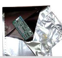
Intercept Technologyの腐食防止フィルムは、従来のように製品に膜を形成して腐食を防止するのではなく、腐食性ガスを中和させる働きのあるフィルムで、腐食の起こらない空気環境を形成します。
Even if a little corrosion occurs in electronic parts, it causes the breakdown. The tolerance of corrosion has become smaller according to integrating and making of the miniaturization parts of the equipment minute. Furthermore, it is not enough in a corrosion control in the production process alone. There are necessities to removes the factor of corrosion by all the processes of the product transport and keeping, and even of keeping the spare parts.
The corrosion prevention film of Intercept Technology is not a film with working to form the film to the product and to prevent corrosion so far but a film to neutralize the causticity gas. It forms the air environment without corrosion.
腐食性ガスによる電子部品の劣化、ハンダ濡れ性の低下
The electronic parts is deteriorated by the corrosive gases
The problem of the wetting balance
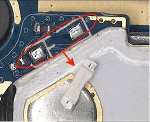 左の写真は、基板実装したLEDユニットが脱落した実例です。下の写真のLEDユニットは日本で射出成形されたのちに、Intercept technologyのフィルムで包装され中国へ送られ、中国の工場で自走されたものです。脱落したLEDユニットを拡大してみましたところ、写真にあるように日本で生産されたLEDユニット端子にはハンダが、しっかりと付着しており良好な状態です。
一方、基板ターミナル部はハンダがターミナルより剥がれ、LED端子側に持っていかれた状態で、基板ターミナルへのハンダ濡れ性に問題がありと示されました。基板の管理、保管時、ターミナル表面に酸化皮膜が形成され、ハンダ濡れ性に問題を起こしたため、LED端子側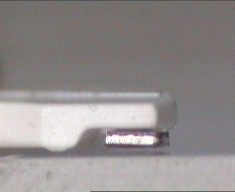 にハンダごと剥がされました。一方のLEDユニットは製造工程から出荷梱包を通じてスタティック・インターセプトにてリードフレーム表面を保護しており、酸化皮膜の形成が無く、ハンダ濡れ性が良好であった。
この基板のターミナルは、銀メッキが施されています。この部分が湿気より硫化水素、二酸化硫黄などの腐食ガスの影響により銀メッキ部分に酸化皮膜が形成されました。中国の上海地区の大気中の硫化水素濃度は約800ppbで日本の100倍以上の汚染度です。大気汚染が腐食の大きな原因です。
In the above photograph, it is the example that the LED unit mounted the substrate drops out. The LED unit in the photograph is the one that is wrapped with the film of Intercept Technology after the shooting molding is done in Japan, sent to China, and mounted in the Chinese factory.
When the LED unit which it drops out is expanded, as shown in the photograph the LED unit terminals produced in Japan is adhered the solder firmly and excellently.
On the other hand, the substrate terminal installed in China whose solder peeled off from the terminal shows the problem of the wetting balance in the substrate terminal. The oxide surface film was formed on the terminal when the substrate was managed and kept, and it had made trouble of the wetting balance in the substrate terminal. That caused peeling off the terminal LED side by the solder. On the other hand the surface of the lead frame was protected during the manufacturing process in the LED unit by Static intercept through the shipment packing, and, the oxide film was not formed, and the solder wetting balance was excellent.
In the terminal of this board, is silver plated. An oxidation film was formed on a silver plating part by hydrogen sulfide, the corrosion gas such as the sulphur dioxide and influence of the moisture. The atmospheric hydrogen sulfide density of Shanghai district in China is about 800ppb. This is more 100 times of pollution degree than Japanese. Air pollution is a big cause of corrosion.
基板回路の抵抗増加防止:基板ターミナルの腐食による回路不良の根絶
Use of in short or prolonged storage of digital devices,
transportation inside and outside the factory and in the clean rooms.
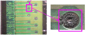 基板ターミナル部分が、腐食ガス(硫化水素、二酸化硫黄など)により腐食が始まると抵抗が増加し、回路不良を誘発させます。
グラフは、7PPBの硫化水素槽に基盤回路を入れて暴露テストを行ない、日毎に抵抗値を測定したものです。保護をしなかった回路(青線)は約1週間で基準値を超え、インターセプトで保護した回路(赤線)は変化がありませんでした。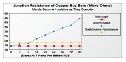
Resistance increases when corrosion starts by the corrosion gas (hydrogen sulfide and sulfur dioxide, etc.), and a defective circuit is caused in the substrate terminal part.
The graphshows that a basic circuit in the hydrogen sulfide tank of 7ppb, does the exposure test, and is measured the resistance every day. The circuit (blue line) not protected exceeded the standard value in about one week. On the other hand, the circuit (red line) protected by Intercept was changeless.
組立工程中や搬送時におこる、静電気によるデバイスの破壊防止と帯電防止
Destruction prevention when in assembler degree and transported of device by static electricity
デジタルデバイスの短長期保管、工場内搬送、輸送、クリーンルーム内などでの使用
Use of in short or prolonged storage of digital devices, transportation inside and outside the factory and in the clean rooms.
 スタティック・インタセプトは他の帯電防止フィルム・シートと違い、溶剤、カーボンなどを含んでいません。温度や湿度による電気抵抗値の変化、ブリード、アウトガス、コンタミが発生する心配のないクリーンなフィルムです。
スタティック・インタセプトは、酸化銅粒子を混入しネットを形成することで安定した電気特性が得られました。
その性能から最先端半導体企業のクリーンルーム100クラスでも使用されています。
この独自原理はCOMOS(Copper Molecular Oxide Semiconductor)と称せられ、同時にAMC(Airborne Molecular Contaminants、浮遊粒子状汚染物質)を吸着し中和する働きがあります。
The static intercepting contains neither the solvent nor the carbon, etc. unlike other electrification prevention film seats. It is a clean film that doesn't make the change of the electrical resistance value, bleeding, the out gas, and the contamination according to the temperature and humidity.
The Static Intercept gets a steady electrical property by mixing the copper oxide particle and the formation net.
This original principle is called COMOS ( Copper Molecular Oxide Semiconductor ), and there is working that adsorbs AMC ( Airborne Molecular Contaminants and a suspended particulate contaminant) and neutralizes them at the same time.
In a100 classes clean room of the state-of-the-art semiconductor enterprise, the Static Intercept is used to the performance.
Application
AT&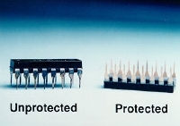 T社、TEXAS INSTRUMENTS社、Honeywell社ほか様々な電子部品メーカーや、電子装置メーカーで採用されています。
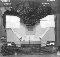
Analogic社では、MRI装置の国内輸送、海外輸出に1998年以来採用されており、静電気破壊などによる事故ゼロです。
It is adopted in the electronic parts manufacturer and the electronic device manufacturer of AT&T Co., TEXAS INSTRUMENTS Co., and Honeywell Co. and others variously.
In the Analogic Co., it is adopted for an inland transport and overseas export of the MRI device since 1998, and there has been no accident of the electrostatic discharge failure etc.
 防錆フィルム